

As electronic circuit boards and components become more powerful and smaller, inherent heat can result in significant damage. Hot spots can be identified by infrared thermography, permitting better thermal management and bigger advances in circuit board design.
Electronic systems designers are trying to find ways to keep their components cool while the sizes of their devices get smaller.
Heat can become a real problem as chips shrink and their densities within components grow, not only for devices which are utilized in civilian life, but also those used in the military. The problem expands beyond inconvenience, to one of safety in the latter instance. In order to maintain the integrity of weapons and communications systems the armed forces depend on the quality of their electronics.
In order to help designers make substantial reductions in electronic component weight, size, and power consumption and thus eliminate the problem of heat dissipation, Government agencies are spending millions to find new thermal management technologies.
Contact Vs. Non-contact Testing
One designer of VXI boards was experiencing a higher than usual flow of returns, with complaints about the boards overheating. The engineers were employing simulation modeling to establish where to add fans and design in heat sinks to dissipate heat.
Additionally, they mounted thermocouples to the board during testing and quality phases, hoping to determine potential design issues. With little result, they finally considered scanning the boards with an infrared camera.
U.S. national sales director for FLIR, Chris Bainter, says infrared has an advantage over thermocouples. “First of all, how do you know where to mount the thermocouples if you don’t know where the hotspots are?” he asks. “Imagine mounting hundreds of probes to a board. It’s unrealistic and not really effective.”
Bainter went to the manufacturing site with an infrared camera. The hot spots were instantly apparent after turning it on and aiming it at a board, and they were nowhere near the fans, heat sinks, or thermocouples.
In that first instant we saw the thermal image, we knew exactly where the hottest points on the board were, and which chips were hotter than anything else.
Chris Bainter, U.S. National Sales Director, FLIR
The first step is knowing where to begin troubleshooting but infrared can also be helpful in designing a circuit board’s thermal management system. The engineers realized their fans and heat syncs were not mounted near the hottest components in this particular board design.
The question was, were they really needed? Or rather, had the engineers designed in additional power draw and weight with thermal management components which were no longer required?
Knowing more about the device’s true thermal properties and heat dissipation can be crucial to improving overall design, enhancing simulation models, and speeding up the fast prototyping phase of the development cycle.
Accounting For Shrinkage
The challenges of heat grow as devices continue to shrink. For instance, imagine going from a VXI board which is roughly 9 ” x 13 ” down to a device the size of a smart phone with individual components a few hundredths of a micron. Components of that size are unable to even accommodate a thermocouple to measure heat.
The answer is to attach an RTD probe, which is smaller than, but similar to, a thermocouple. Yet, even this smaller probe can alter heat measurements by acting as a heat sink.
It’s challenging, maybe impossible, to measure temperature on really small devices with contact forms of temperature measurement. When they get small enough, a probe can affect the thermoresponsivity of the device.
Chris Bainter, U.S. National Sales Director, FLIR
A non-contact form of temperature measurement, like infrared imaging, is needed in these instances. Another common utilization for infrared thermal cameras among electronics designers and manufacturers is detecting hot spots for failure analysis.
FLIR T1K Handheld HD Infrared Camera. Image Credit: FLIR Systems
In this instance, measuring absolute temperatures is not as crucial as locating small hot spots which are causing subtle thermo-differentials. These hot spots can be indicative of troubles with the device or failure points.
While passive thermal imaging works well, a method known as “Lock-In Thermography” can enhance the sensitivity of the camera by over 10 times, making it much more simple to detect subtle, small hot spots. By identifying insufficient solder, infrared inspection can also help with quality assurance.
Insufficient solder heightens the circuit resistance at the solder joint and so, raises the temperature enough to be detected by an infrared camera. A faulty circuit will show up as a different temperature profile from a good one, and that can help to establish if the circuit should pass or fail.
Is Thermography Cost Justifiable?
As electronic components shrink, the cost justification for thermography is growing. Modern infrared cameras provide up to 16 times the resolution of cameras which were employed 10 years ago, for almost the same cost.
Bainter believes that as costs continue to fall, thermal infrared cameras will become a standard thermal measurement tool on every test bench, alongside digital multimeters, voltage analyzers, and oscilloscopes.
Advances in technology will also factor in. Thermal imaging still has opportunities for advancement, where testing in electronics inspection is concerned. Correcting for surface emissivity is one challenge to thermal imaging.
A number of electronic boards possess components with varying emissivities, some of which are shiny, and so, have a low emissivity. This means that they are more challenging to measure for absolute temperatures.
Methods like high emissivity coatings, emissivity mapping, and image subtraction are examples of ways to compensate. In image subtraction, before the device is energized, the infrared inspection system software captures an image in order to create a thermal baseline.
That baseline image is then taken away from subsequent images after the device is turned on, thereby removing the static reflected temperature values, leaving only the true temperature deltas because of the heating of the device.
Image subtraction removes all of the apparent thermal hot spots effectively because of erroneous static reflected temperatures from lower emissivity devices and lets the user focus on true thermal hot spots produced by the device itself.
Attacking Counterfeit Products
There are chances for thermography to advance into new applications, like counterfeit product detection, which is another growing problem in military purchasing.
Phony devices using cheaper materials and knock off designs may have different thermal signatures from the originals, even if on the outside, they look similar.
Chris Bainter, U.S. National Sales Director, FLIR
Via the internet, those devices are available widely at bargain prices, and suspect counterfeit and bogus military-grade electronic parts can be found on many internet purchasing platforms, according to a Government Accountability Office (GAO) study. In fact, during a recent study, none of the vendors supplied to the GAO were legitimate.
The GAO received responses from 396 vendors after submitting requests for quotes, of which 334 were located in China; 25 in the United States; and 37 in other countries, including Japan and the United Kingdom. The GAO chose the first lowest price bids, and all 16 parts were supplied by vendors in China.
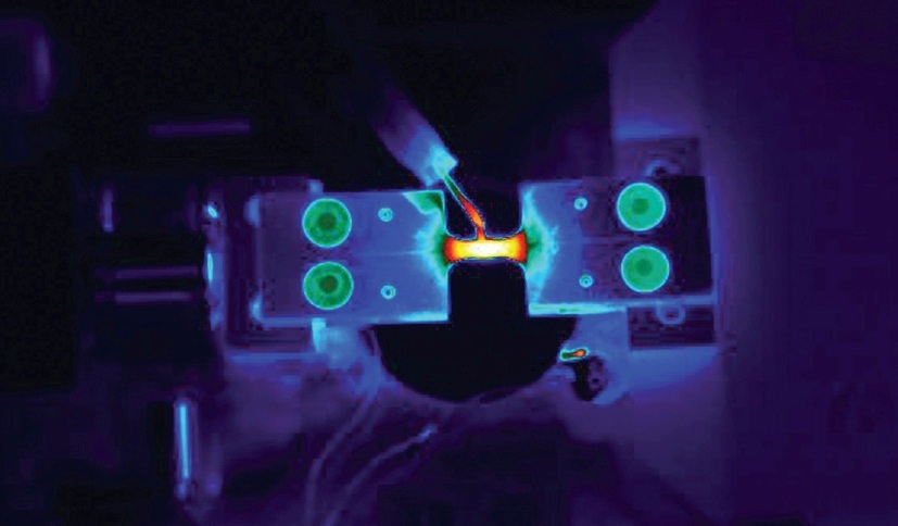
Thermal image of a surface mount thermocouple installed on a material sample. Image Credit: FLIR Systems
The Payoff
With infrared imaging, where the rubber hits the road is testing and identifying problems which once were impossible to find, or at least a challenge to find quickly. For manufacturers, their ROI would be images which pinpoint a design flaw, thus decreasing test times and time-to-market.
A further benefit to thermal imaging is that it enables engineers to view a complete thermal map of the circuit board, with temperature values for each pixel. There is no concern about mounting thermocouples or RTDs in the wrong place, resulting in erroneous readings.
Thermal images show where the hottest points on a board are. Thermal imaging can of course be employed in numerous stages of the research and development process, beyond simple circuit board imaging.
This information has been sourced, reviewed and adapted from materials provided by FLIR Systems.
For more information on this source, please visit FLIR Systems.
"electronic" - Google News
April 30, 2020 at 04:52PM
https://ift.tt/2KS6miF
Comparing Contact vs. Non-Contact Electronic Component Testing - AZoM
"electronic" - Google News
https://ift.tt/39JdyJu
Shoes Man Tutorial
Pos News Update
Meme Update
Korean Entertainment News
Japan News Update
Bagikan Berita Ini


0 Response to "Comparing Contact vs. Non-Contact Electronic Component Testing - AZoM"
Post a Comment